EUV Lithography Equipment: Transformation to Revolutionize the Chip Industry by 2025
EUV Lithography is set to drive the chip miniaturization race, with crucial technological and geopolitical shifts influencing the semiconductor landscape.
In the rapidly evolving semiconductor arena, the EUV Lithography Equipment market is catching the spotlight as it rides the crest of innovation waves towards 2025. As the industry races to miniaturize chips to unprecedented sizes, EUV lithography technology stands as a linchpin, driving demand and catalyzing a projected Compound Annual Growth Rate (CAGR) of 12%. According to macholevante.com, these groundbreaking shifts aren’t without significant technological advancements and geopolitical intricacies.
Surging Demand in the New Era of Chip Miniaturization
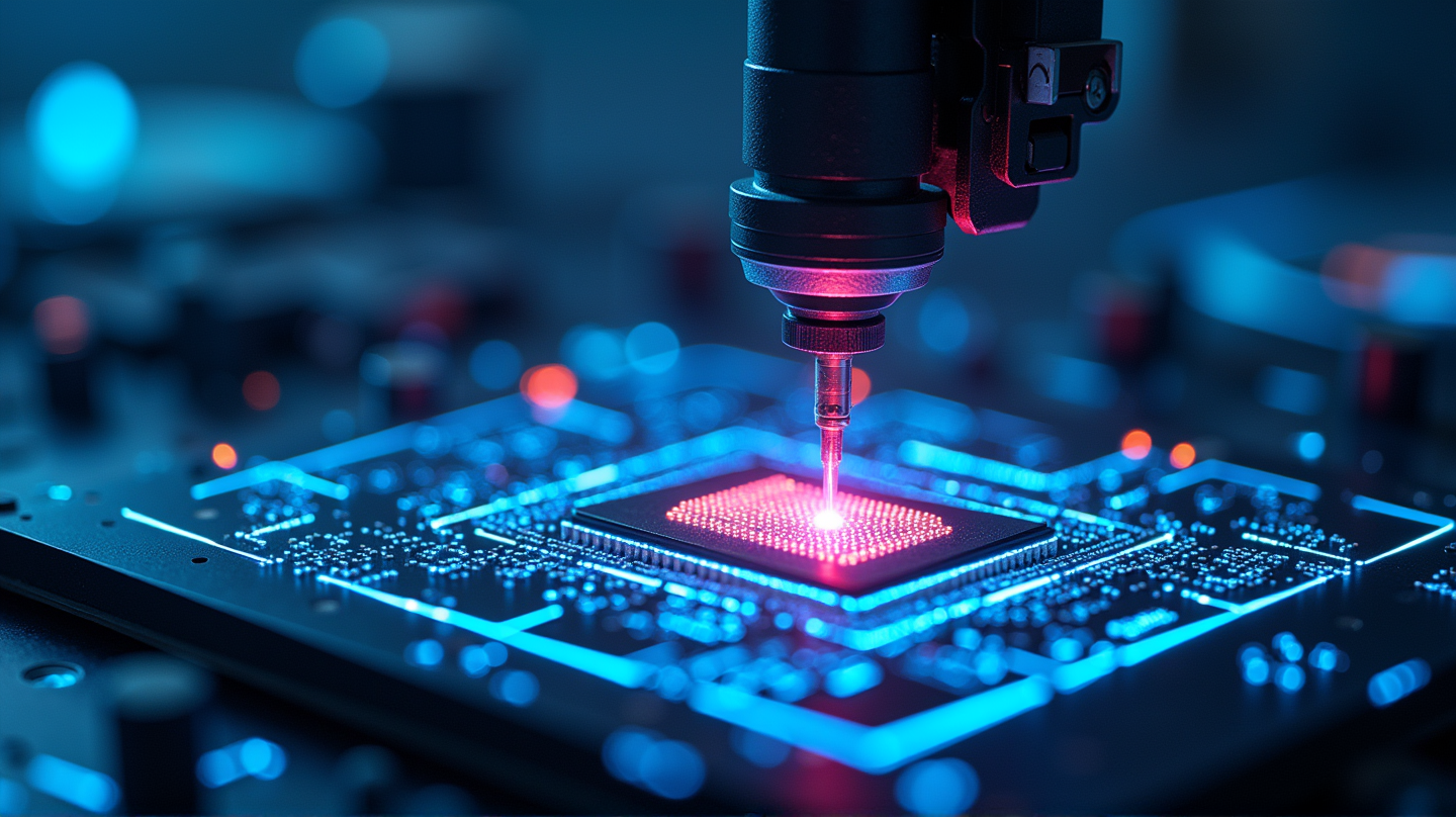
With global consumer electronics, data centers, and the automotive sector pushing boundaries, the need for sub-7nm process nodes is rising. EUV lithography, utilizing a 13.5 nanometer wavelength, promises unparalleled precision in silicon wafer patterning. Companies like ASML Holding NV are at the forefront of this transformation, leveraging systems like the Twinscan NXE to dominate the market with advanced capabilities essential for AI and 5G infrastructure.
Navigating Through Complex Geopolitical Currents
The EUV equipment supply chain is a web of intricacies, demanding collaboration across sectors. Key suppliers such as Carl Zeiss AG and Cymer play vital roles. Yet, geopolitical tensions, especially between the US, China, and the EU, introduce hurdles in distribution and servicing, fundamentally altering market dynamics.
Fueling Technological Potential: Key Trends and Innovators
2025 will witness not only technological evolution but also refinement across the EUV scape. High-NA EUV systems redefine possibilities by enabling closer finishings, venturing into sub-2nm territories. This refinement spearheaded by ASML is reshaping optics, mask infrastructures, and resist materials, creating a cooperative symphony of innovation across the industry. Enhancements in light sources, pushing beyond 500W, are another game-changer, optimizing wafer throughput, vital for cost-efficient production.
Competitive Edge in a Dominated Landscape
While ASML’s stronghold seems unshakeable in 2025 as the unconquered leader, the landscape continually shifts. Canon Inc. and Nikon Corp tiptoe into the EUV realm, but the dominance of ASML, lubricated by strategic partnerships, particularly in optics and laser technology, keeps competitors at bay for now. However, consortia and vendors worldwide are already sketching the blueprints for a new dawn of competition, backed by substantial R&D investments and ambitious state policies.
A Glance Forward in Semiconductor Sovereignty
Anticipated to redefine technological sovereignty, the EUV Lithography Equipment market burgeons as nations fervently seek independence in semiconductor production. Infrastructure expansions and investments tick upward, fueled by innovations in High-NA systems and robust automation, sewing the fabric of semiconductor autonomy.
Conclusion: The Technological Renaissance
The EUV Lithography Equipment market represents a cornerstone for the future of semiconductors. Its growth is not just quantitative but transformative. Aligning with strategic innovations and geopolitical recalibrations, industries and governments alike wave the banner for a seamlessly interconnected future where the only certainty is change.
In reflection, the 2025 EUV lithography landscape is teetering on the edge of an innovative renaissance, a reflection of a world embracing immense potential amid dynamic global plays.